Qualcomm Details Snapdragon 835: Kryo 280 CPU, Adreno 540 GPU, X16 LTE
by Matt Humrick on January 3, 2017 5:00 PM EST- Posted in
- Smartphones
- Snapdragon
- Qualcomm
- Adreno
- Mobile
- Snapdragon 835
- Kryo
CPU
The Kryo 280 CPU inside Snapdragon 835 is the first semi-custom architecture to use ARM’s new "Built on ARM Cortex Technology" license. This license (which we abbreviate as BoC) sits between the traditional Cortex processor license, which grants the vendor access to one of ARM’s stock cores, and the architecture license, which allows the vendor to create a completely custom design that conforms to ARM’s ISA. Over the past three generations, Qualcomm has used all three of these licenses: the Snapdragon 810 implemented stock ARM Cortex-A57 and A53 cores with a processor license, the 820’s fully-custom Kryo cores required an architecture license, and the 835 takes advantage of this new license type.
The BoC license allows Qualcomm to make certain changes to a stock ARM core, thereby, creating a semi-custom core that aligns more closely with its performance and power targets, achieves better integration with its proprietary IP (GPU, DSP, etc.), and is specially tailored to the workloads and applications Qualcomm is targeting. There are parts of the microarchitecture that cannot be altered, however. The decoder width and execution pipelines are off limits, for example, because the amount of redesign would be too extensive. For this reason, many of the possible changes involve branch prediction and instruction fetch in the front end.
For the Kryo 280, Qualcomm uses an octa-core, big.LITTLE configuration with four “performance” cores and four lower-power “efficiency” cores, with semi-custom designs for both clusters. Qualcomm did not disclose which ARM cores serve as the foundation for Kryo 280, but the Cortex-A53 is the obvious choice for the efficiency cores, while the performance cores are likely based on the A72 or A73. As expected, Qualcomm did not go into great detail about what modifications it made, but it did confirm that the memory controllers are a custom Qualcomm design. It’s not clear if it uses ARM’s CCI-550 Cache Coherent Interconnect or its own internal solution, though. The performance cores also get a larger instruction window, which determines the number of instructions that can be executed out of order. This potential performance booster requires modifications to several features, including the reorder buffer and issue queues.
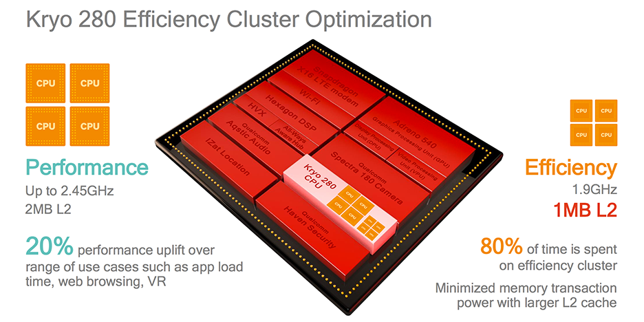
Kryo 280’s efficiency cluster reaches a peak frequency of 1.9GHz, while the performance cluster tops out at 2.45GHz, which seems a bit conservative. According to ARM, the A73 is comfortable running between 2.6GHz to 2.8GHz when using the 14/16nm node. This number could be even higher using Samsung’s new 10nm process, which the Snapdragon 835 uses. There are a few possible explanations that come to mind: Kryo 280’s performance cores are based on the A72 instead of the A73; the changes Qualcomm made, particularly the ones to increase the instruction window size, are limiting the peak frequency; more of the thermal budget is being used for the GPU; or Qualcomm is prioritizing battery life over peak performance. I suspect there’s still some headroom available, leaving the door open for a Snapdragon 835 variant with higher CPU frequencies later this summer.
The Kryo 280’s L2 caches have doubled in size relative to those in the Snapdragon 820. The efficiency cluster uses a 1MB L2 cache, while the performance cluster uses a 2MB L2 cache. The larger caches increase performance and reduce power consumption at the same time by reducing memory traffic, according to Qualcomm.
At this point you’re probably wondering why Qualcomm went the semi-custom route for Snapdragon 835’s CPUs instead of using its custom Kryo architecture? The company said that it considers all of the available options (stock ARM, custom, and now semi-custom) for each generation and selects the best technology. Performance and power are obvious criteria, but other factors like cost, availability, and marketing affect this decision too.
| Qualcomm Snapdragon SoCs: Three Generations | |||
| SoC | Snapdragon 835 (MSM8998) |
Snapdragon 820 / 821 (MSM8996 / MSM8996 Pro) |
Snapdragon 810 (MSM8994) |
| CPU | 4x Kryo 280 Performance @ 2.45GHz 4x Kryo 280 Efficiency @ 1.90GHz |
2x Kryo @ 2.15GHz / 2.34GHz 2x Kryo @ 1.59GHz / 2.19GHz |
4x Cortex-A57 @ 2.00GHz 4x Cortex-A53 @ 1.50GHz |
| GPU | Adreno 540 | Adreno 530 @ 624MHz / 653MHz | Adreno 430 @ 630MHz |
| Memory | 2x 32-bit @ 1866MHz LPDDR4x 29.9GB/s |
2x 32-bit @ 1866MHz LPDDR4 29.9GB/s |
2x 32-bit @ 1600MHz LPDDR4 25.6GB/s |
| ISP/Camera | Dual 14-bit Spectra 180 ISP 1x 32MP or 2x 16MP |
Dual 14-bit Spectra ISP 1x 25MP or 2x 13MP |
Dual 14-bit ISP 1x 21MP |
| Encode/Decode | 2160p30 (2160p60 decode), 1080p120 H.264 & H.265 |
2160p30 (2160p60 decode), 1080p120 H.264 & H.265 |
2160p30 (2160p60 decode), 1080p120 H.264 & H.265 |
| Integrated Modem | Snapdragon X16 LTE (Category 16/13) DL = 1000Mbps 3x20MHz CA, 256-QAM UL = 150Mbps 2x20MHz CA, 64-QAM |
Snapdragon X12 LTE (Category 12/13) DL = 600Mbps 3x20MHz CA, 256-QAM UL = 150Mbps 2x20MHz CA, 64-QAM |
Snapdragon X10 LTE (Category 9) DL = 450Mbps 3x20MHz CA, 64-QAM UL = 50Mbps 1x20MHz CA, 16-QAM |
| Mfc. Process | 10nm LPE | 14nm LPP | 20nm SoC |
GPU
The Snapdragon 835 includes an updated Adreno 540 GPU. It uses the same basic architecture as the Adreno 530 in Snapdragon 820, which accounts for the product number’s small increment. For this generation, Qualcomm focused on optimizing bottlenecks and reducing the amount of work done per pixel by improving depth rejection, for example. The ALUs and register files also received some attention, although, nothing specific was mentioned.
The Adreno 540 performs higher-order texture filtering at lower cost relative to previous designs, processing 16 texels/clock for trilinear filtering. For comparison, ARM’s Mali-G71 processes 1 bilinear filtered texel per clock, or 1 trilinear filtered texel over 2 clocks, per core. So a 16 core configuration (MP16) is capable of 16 texels/clock (bilinear) but only 8 texels/clock (trilinear).
According to Qualcomm, the Adreno 540 sees a 25% increase in 3D rendering performance relative to the Adreno 530 in Snapdragon 820. It’s not clear how much of this is due to architectural improvements, however, because the peak GPU frequency is not official; initial clues point to a modest frequency boost for the GPU, although not enough to account for the claimed 25% increase in performance.
The Adreno 540 supports the latest graphics APIs, including OpenGL ES 3.2, DirectX 12, and Vulkan. It also includes full support for OpenCL 2.0 and Renderscript.
DSP & ISP
Hexagon 680 DSP
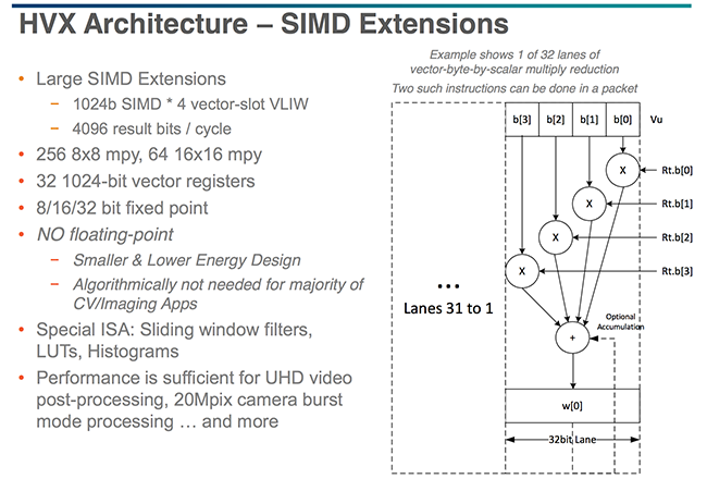
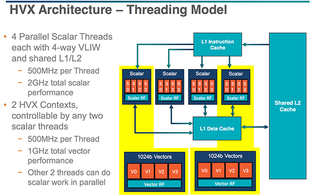
Last year, Qualcomm introduced a completely new architecture for the Hexagon 680 DSP in Snapdragon 820, featuring its new Hexagon Vector eXtensions (HVX) specifically designed for advanced photo and video processing, virtual reality, and computer vision workloads. The Hexagon 680 can work on two vector threads in parallel using two HVX contexts, each containing four 1024-bit SIMD pipelines, which are significantly wider than the 64-bit SIMD NEON pipelines typically found in ARM CPUs, allowing each HVX context to work on 4,096 bits/cycle compared to 128 bits/cycle for a single CPU core.
In addition to the two HVX contexts for vector instructions, the Hexagon 680 also contains four threads for scalar instructions, each with 4 VLIW pipelines. Scalar and vector instructions can be processed in parallel too, using two scalar threads and two vector threads. This allows concurrent execution of audio and imaging tasks, because the scalar threads generally handle audio and voice processing.
Hexagon 680 DSP
While the Hexagon 680 DSP uses a multithreaded programming model similar to a CPU, it’s still a specialized processor designed to accelerate specific workloads involving streaming data. It’s meant to work alongside the CPU and GPU rather than replace them. For example, in order to reduce die space and power consumption, it only performs integer and not floating point operations. This specialization gives the DSP a significant performance and power advantage over the CPU for certain tasks.
Qualcomm did not discuss the updated Hexagon 682 DSP in Snapdragon 835 in much detail, but considering the big changes last year and the small increment in the product number, it’s likely the Hexagon 682’s architecture looks very similar to what’s summarized above.
The Snapdragon 835, like the 820, contains two additional DSP cores. One performs signal processing in the X16 LTE modem. The other is a special low-power DSP core Qualcomm calls the All-Ways Aware Hub. This lives on a separate power island and connects to a range of different sensors. With support for the Google Awareness API, it enables low-power activity tracking, such as step counting, and positioning using LTE, Wi-Fi, and Bluetooth LE. As the name implies, this DSP is always active, feeding contextual data from sensors to various apps and allowing the more complex, compute-focused Hexagon DSP to power down.
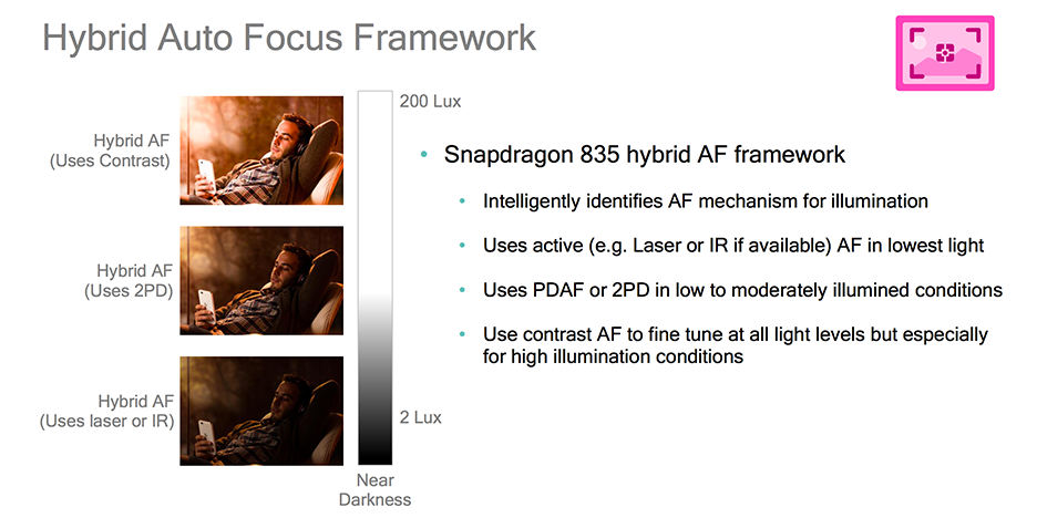
Also packed inside the Snapdragon 835 is an updated ISP. The Spectra 180 is a dual 14-bit ISP that supports up to a 32MP single camera or two 16MP cameras, which is an increasingly important feature for flagship phones. The ISP gains enhanced support for hybrid autofocus systems, which select the best AF method based on lighting conditions. It also supports dual photodiode phase-detect autofocus (2PDAF), which splits each pixel (typically a larger 1.4µm pixel) into two photodiodes: one for image capture and one for phase detection. By using every pixel for phase detection, AF performance is significantly improved, focusing up to twice as fast as PDAF in low-light conditions.
The Spectra 180 ISP also gains a fixed-function block to perform hardware accelerated zig-zag HDR (zzHDR), an HDR imaging technique that diagonally interleaves lines of pixels with long and short exposures in a zig-zag pattern. zzHDR can be used to show a live preview of the HDR image, record HDR video, or capture HDR photos without any shutter lag, but sacrifices some image resolution.


58 Comments
View All Comments
colinisation - Saturday, January 7, 2017 - link
I think the custom core buzz was because Qualcomm beat outgeneric ARM cores in the past - think Cortex A8/9 vs Scorpion but also Cortex A15/57 lest a bad taste in peoples mouths when compared to Apple's cores at the time and the popular refrain was "its because they are generic ARM cores". I however thinks things have moved on since then and ARM has poured more resources into their custom cores and A72/73 are more focused on mobile as opposed to being a bridge to the server world.I agree with you on the common workloads front - have you got any links for the claim on Kirin 960 vs 8890. I know Huawei are trumpeting their Cortex M7 integration.
I think in order to properly bench these things you would need to dismatle phone connect it up to a voltmeter and power source to determine how much power is being draw then run it through a number of scenarios - web browsing, gaming, app installs etc Before measuring power draw, app opening speed, performance, responsiveness and then calculate how long it will last given its battery size. This is a LOT of work and not sure its reasonable to ask review sites to put that much time into 1 review
lilmoe - Sunday, January 8, 2017 - link
The Cortex A9 was significantly faster than Scorpion. It wasn't until Krait that Snapdragons really closed the gap, barely. Krait Snapdragons benched better, but Cortex A9 Exynos processors were simply faster and more fluid running as a whole (they got a bit toastier at times though)."I think in order to properly bench these things you would need to dismatle phone connect it up to a voltmeter and power source"
I wish it were that simple. You just can't build a conclusion on any sort of systematic/synthetic test. Even if it were a browser script which is supposed to simulate "real life". Browsing habits differ by user, and the browser used and the governer the OEM implements (among other "secret sauce" ingredients) make a bigger impact than processor efficiency on the readings of your measuring equipment and/or on overall system battery life.
"have you got any links for the claim on Kirin 960 vs 8890"
My opinions are generally made from personal, real life experience. I have lots of friends that try out different phones and we usually spend hours comparing.
But technically speaking, do we really need proof? There's one fact that EVERYONE fails to realize (especially Andre here, the rest of Anandtech don't seem to care); ALL of these processors are mainly running on the small cluster!!! Both the Kirin and Exynos are mostly running on the same 4 Cortex A53 cores. The big/performance cluster works for split seconds and goes back to sleep, mostly when loading a page, or launching an app.
That being said, there are 2 main things that make Exynos SoCs better than Helios and Kirins IMO:
1) The interconnects and co-processors are simply better. Samsung's fixed function video decoder, in particular, is industry leading in performance and efficiency (it's been this way since the Hummingbird in my experience).
2) Two of the M1 cores are always offline. They don't come online unless needed. Not sure how much this makes an impact, but the Kirin has all 8 online at all times.
A simple Youtube search shows lots of battery tests between the Exynos GS7 Edge and the Mate 9. The GS7 has better battery life even with a smaller battery.
I won't be upgrading my GS7 until we see an upgrade to the A53 core.
SarahKerrigan - Tuesday, January 3, 2017 - link
Is Kryo 280 definitely a Cortex derivative? It seems really weird that they'd call it a Kryo instead of stating outright that it was an enhanced A73 or something...shabby - Tuesday, January 3, 2017 - link
Probably don't want to admit that the a73 is better than their offering so they went this route and used a slightly tweaked a73 and don't have to divulge any other info about it.prisonerX - Wednesday, January 4, 2017 - link
The terms of the licence dictate that it is indeed a Cortex derivative, and almost all Cortex. The name is pure marketing.name99 - Wednesday, January 4, 2017 - link
More interesting is the issue of what this means for the QC Server chip.Did QC conclude there's more money and less competition in ARM servers, so moved the Kryo team there? Because this movie certainly seems to suggest that they've given up trying to really compete in the ARM CPU space --- now they'll just compete, presumably, on the basis of Hexagon, Adreno, and wireless, but with essentially the same CPU as everyone else?
prisonerX - Wednesday, January 4, 2017 - link
It could just be priorities and the fact they can't do better than ARM's design in the short/medium term. ARM's design may be getting better as they bring more resources to bear or the design cycles too long at this point to have their own design.The server space is ripe for "disruption." Desktops and PCs generally are slowly going the way of the dodo and the future is mobiles and servers. People aren't going to let Intel keep such a strategic segment all to themselves. Single thread performance is flat and power consumption is king and they know Intel is vulnerable. The hyenas are nipping at the wounded and bleeding former lion king.
lilmoe - Wednesday, January 4, 2017 - link
Or it simply means that instead of focusing solely on how to achieve the highest brute performance for a given TDP, one should focus more on efficiency of a specific performance target and work more on offloading more tasks to dedicated blocks and co-processors that the very best CPU architecture can never dream to achieve.Which is exactly what they did, and what I believe is the right thing to do. You guys are focused on the wrong thing for the wrong form factor. This isn't desktop computing. Heck, even desktop CPUs are moving in that direction. After a certain performance threshold, CPUs get less and less important.
lilmoe - Thursday, January 5, 2017 - link
And just to add something I've been saying over and over for a while. What Qualcomm, Samsung and ARM should be focusing on from this point is NOT the high performance cluster, but the efficiency cluster. The A53 is in dire need for a refresh. If you guys want to focus on the CPU aspect, you need to start focusing on this. Qualcomm are saying that the small cluster is handling 80% of the workload alone; I say 90%. That 1MB of L2 they slapped on the small cluster might mean all the difference they needed on the CPU side.jospoortvliet - Thursday, January 5, 2017 - link
Well there is the a35 already...