Qualcomm Demos 48-Core Centriq 2400 Server SoC in Action, Begins Sampling
by Anton Shilov on December 16, 2016 6:00 PM EST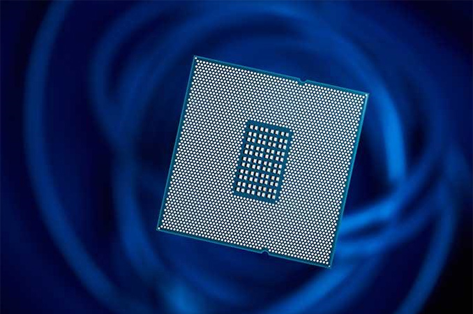
Qualcomm this month demonstrated its 48-core Centriq 2400 SoC in action and announced that it had started to sample its first server processor with select customers. The live showcase is an important milestone for the SoC because it proves that the part is functional and is on track for commercialization in the second half of next year.
Qualcomm announced plans to enter the server market more than two years ago, in November 2014, but the first rumors about the company’s intentions to develop server CPUs emerged long before that. In fact, being one of the largest designers of ARM-based SoCs for mobile devices, Qualcomm was well prepared to move beyond smartphones and tablets. However, while it is not easy to develop a custom ARMv8 processor core and build a server-grade SoC, building an ecosystem around such chip is even more complicated in a world where ARM-based servers are typically used in isolated cases. From the very start, Qualcomm has been rather serious not only about the processors themselves but also about the ecosystem and support by third parties (Facebook was one of the first companies to support Qualcomm’s server efforts). In 2015, Qualcomm teamed up with Xilinx and Mellanox to ensure that its server SoCs are compatible with FPGA-based accelerators and data-center connectivity solutions (the fruits of this partnership will likely emerge in 2018 at best). Then it released a development platform featuring its custom 24-core ARMv8 SoC that it made available to customers and various partners among ISVs, IHVs and so on. Earlier this year the company co-founded the CCIX consortium to standardize various special-purpose accelerators for data-centers and make certain that its processors can support them. Taking into account all the evangelization and preparation work that Qualcomm has disclosed so far, it is evident that the company is very serious about its server business.
From the hardware standpoint, Qualcomm’s initial server platform will rely on the company’s Centriq 2400-series family of microprocessors that will be made using a 10 nm FinFET fabrication process in the second half of next year. Qualcomm does not name the exact manufacturing technology, but the timeframe points to either performance-optimized Samsung’s 10LPP or TSMC’s CLN10FF (keep in mind that TSMC has a lot of experience fabbing large chips and a 48-core SoC is not going to be small). The key element of the Centriq 2400 will be Qualcomm’s custom ARMv8-compliant 64-bit core code-named Falkor. Qualcomm has yet has to disclose more information about Falkor, but the important thing here is that this core was purpose-built for data-center applications, which means that it will likely be faster than the company’s cores used inside mobile SoCs when running appropriate workloads. Qualcomm currently keeps peculiarities of its cores under wraps, but it is logical to expect the developer to increase frequency potential of the Falkor cores (vs mobile ones), add support of L3 cache and make other tweaks to maximize their performance. The SoCs do not support any multi-threading or SMP technologies, hence boxes based on the Centriq 2400-series will be single-socket machines able to handle up to 48 threads. The core count is an obvious promotional point that Qualcomm is going to use over competing offerings and it is naturally going to capitalize on the fact that it takes two Intel multi-core CPUs to offer the same amount of physical cores. Another advantage of the Qualcomm Centriq over rivals could be the integration of various I/O components (storage, network, basic graphics, etc.) that are now supported by PCH or other chips, but that is something that the company yet has to confirm.

From the platform point of view, Qualcomm follows ARM’s guidelines for servers, which is why machines running the Centriq 2400-series SoC will be compliant with ARM’s server base system architecture and server base boot requirements. The former is not a mandatory specification, but it defines an architecture that developers of OSes, hypervisors, software and firmware can rely on. As a result, servers compliant with the SBSA promise to support more software and hardware components out-of-the-box, an important thing for high-volume products. Apart from giant cloud companies like Amazon, Facebook, Google and Microsoft that develop their own software (and who are evaluating Centriq CPUs), Qualcomm targets traditional server OEMs like Quanta or Wiwynn (a subsidiary of Wistron) with the Centriq and for these companies having software compatibility matters a lot. On the other hand, Qualcomm’s primary server targets are large cloud companies, whereas server makers do not have their samples of Centriq yet.
During the presentation, Qualcomm demonstrated Centriq 2400-based 1U 1P servers running Apache Spark, Hadoop on Linux, and Java: a typical set of server software. No performance numbers were shared and the company did not open up the boxes so not to disclose any further information about the CPUs (i.e., the number of DDR memory channels, type of cooling, supported storage options, etc.).
Qualcomm intends to start selling its Centriq 2400-series processors in the second half of next year. Typically it takes developers of server platforms a year to polish off their designs before they can ship them, normally it would make sense to expect Centriq 2400-based machines to emerge in the latter half of 2H 2017. But since Qualcomm wants to address operators of cloud data-centers first and companies like Facebook and Google develop and build their own servers, they do not have to extensively test them in different applications, but just make sure that the chips can run their software stack.
As for the server world outside of cloud companies, it remains to be seen whether the server industry is going to bite Qualcomm’s server platform given the lukewarm welcome for ARMv8 servers in general. For these markets, performance, compatibility, and longevity are all critical factors in adopting a new set of protocols.
Related Reading:
- Evaluating Futuremark's Servermark VDI on the Supermicro SYS-5028D-TN4T
- New GIGABYTE Server Motherboards Show Xeon D Round 2
- AMD Exits Dense Microserver Business, Ends SeaMicro Brand
Source: Qualcomm


88 Comments
View All Comments
Kevin G - Monday, December 19, 2016 - link
(a) A couple of those years are high level design improvements on paper. With Intel's tick-tock cadence (now design, optimize, process), they much of what is put into these early stages is actually form the previous generation chip they're currently working on but couldn't get working/expected to validate before deliverable time table. This was also mainly between ticks as the tocks were just shrinks of the ticks. Also much like ARM, Intel has different teams working on different chip functions that get put together for an end chip. Memory controller design teams are different from GPU which are different from CPU etc. These may have different design cadences.The big 800 lbs. gorilla in the room is that Intel owns its fabs and directly feeds in process optimization design rules directly into their logic design teams. ARM, QC, and others are at the mercy of outside foundries for this information. Thankfully this information flow starts well before a production node is ready for production. Raw data here is hard to come by but it is believed that this information exchange happens a bit later in the design process than what gets fed into Intel's logic design teams.
(b) This what really optimizes its production line up for. Intel does know when to charge outrageous premiums *cough* 10 core i7 *cough* and it knows when to subsidize to get market share like with Atom. The problem is that this can create conflicts with their otherwise profit maximizing line up. This is why Xeon D is a soldered part and sold mainly to OEMs and companies doing private designs like Facebook and Google. This was purely to prevent ARM from gaining a foothold in the datacenter in the low power sector. Intel would rather these companies purchase more expensive Xeon E5s.
The real chaos has always been getting into mobile for Intel. The only issue for Atom is that at the power levels needed for a phone, ARM was surprisingly competitive performance wise. Intel's pricing of Atom wasn't bad but it didn't offset the software costs in porting/validation x86 plus the need to actively support both x86 and ARM handsets. Intel also failed to indicate that they were willing to continue to provide chips at those prices long term. It seemed that everyone knew that this was a market share strategy and as soon as Intel had their foothold, chip prices would climb.
chlamchowder - Friday, December 16, 2016 - link
No? The article compared the Atom Z2760 and Tegra 3. The Z2760 is Intel's now old Saltwell architecture, on 32nm. The Tegra 3 is on 40 nm. Not sure how far those are apart.But going beyond that, what ultimately matters is who's more power efficient. If Intel's more power efficient on 22 nm than ARM is on 32 nm, Intel wins. Nobody will buy ARM just because it did an admirable job on 32 nm and didn't lose too badly to a 22 nm chip.
witeken - Friday, December 16, 2016 - link
BTW, AnandTech also did a follow-up several months later. http://www.anandtech.com/show/6536/arm-vs-x86-the-...beginner99 - Saturday, December 17, 2016 - link
Yeah the Atom clearly won that and considering that this was the old crappy Atom and not the new one...ddriver - Saturday, December 17, 2016 - link
the old crappy atom vs the new crappy atom lolWilco1 - Saturday, December 17, 2016 - link
The 2nd article compared more like for like CPUs but had the same flaws - both used hardware modifications done by Intel and focussed on tiny JS and browsing benchmarks so it was more a browser efficiency comparison rather than a CPU efficiency comparison. There are still large differences between various JIT compilers today, including between different versions of the same browser.Gondalf - Sunday, December 18, 2016 - link
What a boring discussion. There is a general consensus the ISA doesn't add or sottract power consumption. Intel has decoders, ARM has a longer code to run. At the end all ISAs have their pros and cons.It's all a matter of good od bad process integration of the blue prints.
Wilco1 - Sunday, December 18, 2016 - link
No, the ISA certainly matters, not only in design and validation time, but also PPA (power performance and area). So there is absolutely no difference between say the x87 FPU and the SSE FP instruction set?Intel couldn't make Atom competitive despite their huge process advantage and many billions spent (so don't claim it was for lack of trying). Even the latest Goldmont is about as fast as phones were almost 2 years ago despite a 10W TDP...
Gondalf - Sunday, December 18, 2016 - link
Your answer needs of a good debugging :). You don't say anything to prove your claims about the smoky ARM architecture advantage and you do the mistake to mix a standard Intel 14nm LP (4Ghz at 1V) with Intel 14nm for SOCs (3GHz at 1V).Silvermont was 1-1.5W/core on SOC process and 3-4W/core on the plain LP process for high clock speeds.
Come on Wilco :)
Wilco1 - Sunday, December 18, 2016 - link
Hmm, you didn't answer my question about x87/SSE. Neither you didn't mention anything to prove your incorrect assertion that ISA does have no impact on power consumption.And no I didn't make any mistake about process either. There is no doubt Intel 14nm processes are better than Samsung 16nm. Yet the very latest Atom looks bad compared to an old Galaxy S6. Also you do realise there are several 4-thread Skylake SKUs which have a similar or lower TDP, right?