Assessing IBM's POWER8, Part 1: A Low Level Look at Little Endian
by Johan De Gelas on July 21, 2016 8:45 AM ESTInside the Beast(s)
When the POWER8 was first launched, the specs were mind boggling. The processor could decode up to 8 instructions, issue 8 instructions, and execute up to 10 and all this at clockspeed up to 4.5 GHz. The POWER8 is thus an 8-way superscalar out of order processor. Now consider that
- The complexity of an architecture generally scales quadratically with the number of "ways" (hardware parallelism)
- Intel's most advanced architecture today - Skylake - is 5-way
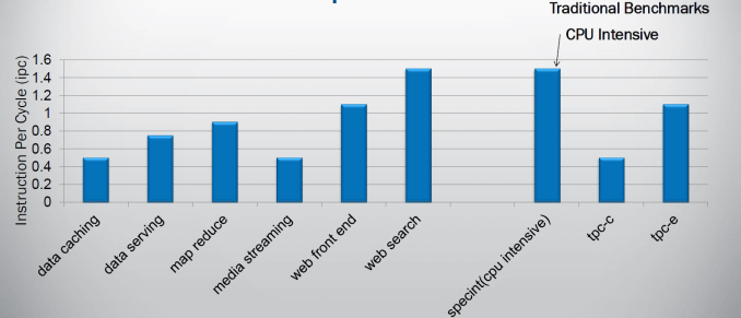
and you know this is a bold move. If you superficially look at what kind of parallelism can be found in software, it starts to look like a suicidal move. Indeed on average, most modern CPU compute on average 2 instructions per clockcycle when running spam filtering (perlbench), video encoding (h264.ref) and protein sequence analyses (hmmer). Those are the SPEC CPU2006 integer benchmarks with the highest Instruction Per Clockcycle (IPC) rate. Server workloads are much worse: IPC of 0.8 and less are not an exception.
It is clear that simply widening a design will not bring good results, so IBM chose to run up to 8 threads simultaneously on their core. But running lots of threads is not without risk: you can end up with a throughput processor which delivers very poor performance in a wide range of applications that need that single threaded speed from time to time.
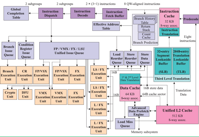
The picture below shows the wide superscalar architecture of the IBM POWER8. The image is taken from the white paper "IBM POWER8 processor core architecture", written by B. Shinharoy and many others.
The POWER8+ will have very similar microarchitecture. Since it might have to face a Skylake based Xeon, we thought it would be interesting to compare the POWER8 with both Haswell/Broadwell as Skylake.
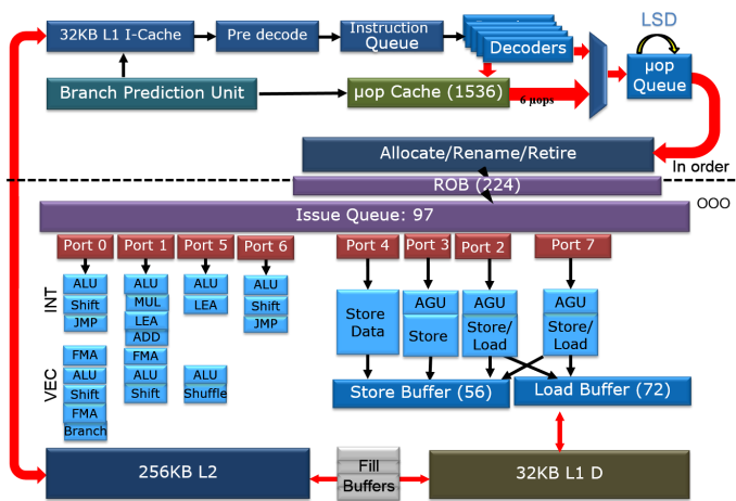
The second picture is a very simplified architecture plan that we adapted from an older Intel Powerpoint presentation about the Haswell architecture, to show the current Skylake architecture. The adaptations were based on the latest Intel optimization manuals. The Intel diagram is much simpler than the POWER8's but that is simply because I was not as diligent as the people at IBM.
It is above our heads to compare the different branch prediction systems, but both Intel and IBM combine several different branch predictors to choose a branch. Both make use of a very large (16 K entries) global branch history table. Both processors scan 32 bytes in advance for branches. In case of IBM this is exactly 8 instructions. In case of Intel this is twice as much as it can fetch in one cycle (16 Bytes).
On the POWER8, data is fetched from the L2-cache and then predecoded into the L1-cache. Predecoding includes adding branch, exception, and grouping. This makes sure that predecoding is out the way before the actual computing ("Von Neuman Cycle") starts.
In Intel Haswell/Skylake, instructions are only predecoded after they are fetched. Predecoding performs macro-op fusion: fusing two x86 instructions together to save decode bandwidth. Intel's Skylake has 5 decoders and up to 5 µop instructions are sent down the pipelines. The current Xeon based upon Broadwell has 4 decoders and is limited to 4 instructions per clock. Those decoded instructions are sent into a µ-op cache, which can contain up to 1536 instructions (8-way), about 100 bits wide. The hitrate of the µop cache is estimated at 80-90% and up to 6 µops can be dispatched in that case. So in some situations, Skylake can run 6 instructions in parallel but as far as we understand it cannot sustain it all the time. Haswell/Broadwell are limited to 4. The µop cache can - most of the time - reduce the branch misprediction penalty from 19 to 14.
Back to the POWER8. Eight instructions are sent to the IBM POWER8 fetch buffer, where up 128 instructions can be held for two thread(s). A single thread can only use half of that buffer (64 instructions). This method of allocation gives each of two threads as much resources as one (i.e. no sharing), which is one of the key design philosophies for the POWER8 architecture.
Just like in the x86 world, the decoding unit breaks down the more complex RISC instructions into simpler internal instructions. Just like any modern Intel CPU, the opposite is also possible: the POWER8 is capable of fusing some combinations of 2 adjacent instructions into one instruction. Saving internal bandwidth and eliminating branches is one of the way this kind of fusion increases performances.
Contrary to the Intel's unified queue, the IBM POWER has 3 different issue queues: branch, condition register, and the "Load/Store/FP/Integer" queue. The first two can issue one instruction per clock, the latter can send off 8 instructions, for a combined total of 10 instructions per cycle. Intel's Haswell-Skylake cores can issue 8 µops per cycle. So both the POWER8 and Intel CPU have more than ample issue and execution resources for single threaded code. More than one thread is needed to really make use of all those resources.
Notice the difference in focus though. The Intel CPU has half of the load units (2), but each unit has twice the bandwidth (256 bit/cycle). The POWER8 has twice the amount of load units (4), but less bandwidth per unit (128 bit per cycle). Intel went for high AVX (HPC) performance, IBM's focus was on feeding 2 to 8 server threads. Just like the Intel units, the LSUs have Address Generation Units (AGUs). But contrary to Intel, the LSUs are also capable of doing simple integer calculations. That kind of massive integer crunching power would be a total waste on the Intel chip, but it is necessary if you want to run 8 threads on one core.


124 Comments
View All Comments
DomOfSF - Thursday, July 21, 2016 - link
Johan de Gelas: blowing minds and educating "the rest of us" since...I dunno, a really long time ago (especially in internet years). Great job on the data, but the real good stuff is in your thoughts and analysis. Thank you!close - Saturday, July 23, 2016 - link
Over a decade...JohanAnandtech - Thursday, July 28, 2016 - link
13 years in the server business, 18 years now of reviewing hardware :-). Thx !!jamyryals - Thursday, July 21, 2016 - link
It seems to me, Intel's focus on bringing their CPU architecture design all the way down to 5W is the reason IBM is able to stand out against them. Intel is focused on creating a scalable architecture while IBM can throw the whole kitchen sink at the server market.Fascinating article, I really enjoyed it.
smilingcrow - Thursday, July 21, 2016 - link
Intel has plenty of unique features in their server platforms which aren't in the consumer platforms so I don't think that is the issue.jospoortvliet - Tuesday, July 26, 2016 - link
The basic design of the core still is the same so there is probably at least some truth in the statement of Jamy.Kevin G - Wednesday, July 27, 2016 - link
Up until this point. Consumer SkyLake and server SkyLake are going to be two different designs. They're certainly related but server SkyLake will have 512 KB of L2 cache per core and support AVX-512 instructions.Server SkyLake is also going to support 3D Xpoint DIMMs, though that difference is more with the platform/chipset than the actual CPU core.
floobit - Thursday, July 21, 2016 - link
Very interesting. It seems odd to me that they chose to configure it in a 2U - except for big data clusters, most of the market space I see this playing is dominated by FC to a SAN. Is this a play in the big data cluster space, or the more traditional AIX/DB2/big iron that IBM has owned for so long?Some questions I'd have:
what virtualization is possible with this architecture? presumably just the standard PowerVM? How well does that work?
What is the impact of IO latency? Could you throw a P3700 or two in here?
JohanAnandtech - Thursday, July 21, 2016 - link
2U: Besides big data storage needs, I suspect 2U is necessary for adequate cooling for the POWER8 chip.Virtualization: Linux KVM works well as far as I know.
We actually tried out a P3700 in there (see: http://www.anandtech.com/show/9567/the-power-8-rev... ) and it worked very well. I asked IBM what a customer should expect when using third party storage (probably no support, but how about waranty?) but no answer yet.
mystic-pokemon - Friday, July 22, 2016 - link
Hi Johan2U is not necessary for cooling a POWER 8 Chip. We do that better with our Barreleye (1.25 OU design). Even storage wise Barreleye has 15 Disk storage bay that can be seen in below links.
http://www.v3.co.uk/v3-uk/news/2453992/google-and-...
Let me know if you wanna ever benchmark a Barreleye. What specific POWER8 proc are you benchmarking with ? (Turismo?). I believe it does slightly better than S812LC on many benchmarks based on the variant of power8 proc S812LC runs.